Detailed P-Channel MOSFET (Datasheet)
Description
Datasheet-driven P-channel MOSFET model for high-side and complementary switch applications.
What you get
- Same workflows as the detailed N-channel model, now preset with P-channel polarity.
- Three user-supplied nonlinear capacitances C_{GD} , C_{GS} , C_{DS} that you can extract from datasheet C_{ISS} , C_{OSS} , and C_{RSS} curves (use C_{GS} = C_{ISS} - C_{RSS} and C_{DS} = C_{OSS} - C_{RSS} ).
- A body-diode characteristic table for the intrinsic source-to-drain diode.
- Transfer and output characteristic matrices to capture datasheet plots of I_D vs V_{GS} and I_D vs V_{DS} .
- Initial condition fields to preload V_{GS} and V_{DS} at simulation start.
Preparing your datasheet data
- Record the transfer curve as |I_D| vs |V_{GS}| at a fixed |V_{DS}| . Enter the magnitudes exactly as read; the model applies the P-channel polarity automatically.
- Capture the output characteristic |I_D| vs |V_{DS}| for a representative |V_{GS}| . Use positive magnitudes even if the datasheet plots negative voltages.
- Populate
Ciss,Coss, andCrsswith either single values or |V_{DS}| -dependent tables. Interpolation is performed if the voltage grids differ. - For the body-diode matrix, provide source-to-drain voltage and current magnitudes describing forward conduction when the source is at the higher potential.
- Set
VgsInitandVdsInitto the actual signed voltages you expect at t = 0 ; for example,-12V on the gate keeps the device off in a high-side switch.
Validation
Start with the default curves, then overlay your own measured datasets. Make sure the tables are monotonic to keep the simulation stable.
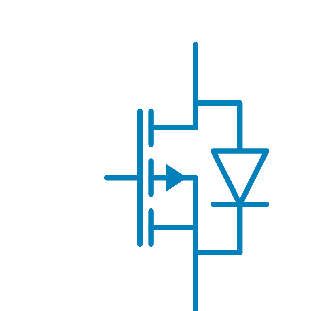
Reading the symbol
- The gate arrow points out of the channel, highlighting P-channel conduction.
- The body diode is flipped relative to the N-channel symbol so current flows from source to drain when forward biased.
- A small bubble on the gate reminds you that the device turns on when the gate is pulled low with respect to the source.
Drop the device anywhere you would normally place the N-channel version; the pins (Drain, Source, Gate) follow the same naming conventions so you can replace one device with the other in existing schematics.
Library
Electrical > Semiconductors
Parameters
| Property | Display Name | Parameter Type | Description |
|---|---|---|---|
| ChannelType | ChannelType | StringParameter | MOSFET channel type (locked to "P" for the solver) |
| Rg | Rg [Ohm] | DoubleParameter | Gate internal resistance value, in Ohm |
| VgsIdMatrix | Transfer Characteristic |Id|[A] vs |Vgs|[V] | DoubleMatrixParameter | Drain-source current magnitude [A] vs. gate-source voltage magnitude [V] |
| VgsIdMatrix_Vds | Transfer Characteristics |Vds| [V] | DoubleParameter | |Vds| value corresponding to the Id vs Vds data |
| VdsIdMatrix | Output Characteristics |Id|[A] vs |Vds|[V] | DoubleMatrixParameter | Drain-source current magnitude [A] vs drain-source voltage magnitude [V] |
| VdsIdMatrix_Vgs | Output Characteristics |Vgs| [V] | DoubleParameter | |Vgs| value corresponding to the Id vs Vds data |
| Ciss | Input Capacitance Ciss[F] vs |Vds|[V] | DoubleMatrixParameter | Input capacitance Ciss[F] vs |Vds|[V] |
| Coss | Output Capacitance Coss[F] vs |Vds|[V] | DoubleMatrixParameter | Output capacitance Coss[F] vs |Vds|[V] |
| Crss | Reverse Transfer Capacitance Crss[F] vs |Vds|[V] | DoubleMatrixParameter | Reverse transfer capacitance Crss[F] vs |Vds|[V] |
| VgsInit | Initial Vgs Voltage [V] | DoubleParameter | Initial Vgs capacitor voltage, in V (signed) |
| VdsInit | Initial Vds Voltage [V] | DoubleParameter | Initial Vds capacitor voltage, in V (signed) |
| Vsd_Is_BodyDiodeMatrix | Body Diode |Isd|[A] vs |Vsd|[V] | DoubleMatrixParameter | Source-drain current magnitude vs source-drain voltage magnitude (body diode) |
Pins
| Property | Pin Name | Type | Description |
|---|---|---|---|
| Drain | Drain | Electrical | Drain |
| Source | Source | Electrical | Source |
| Gate | Gate | Electrical | Gate (Control Input) |
Default Size
| Width | Height |
|---|---|
| 4 | 6 |